- 您现在的位置:买卖IC网 > Sheet目录508 > SI2306BDS-T1-GE3 (Vishay Siliconix)MOSFET N-CH 30V 3.16A SOT23-3
Si2306BDS
Vishay Siliconix
SPECIFICATIONS T A = 25 °C, unless otherwise noted
Limits
Parameter
Symbol
Test Conditions
Min.
Typ.
Max.
Unit
Static
Drain-Source Breakdown Voltage
Gate-Threshold Voltage
V (BR)DSS
V GS(th)
V GS = 0 V, I D = 250 μA
V DS = V GS , I D = 250 μA
30
1.0
3.0
V
Gate-Body Leakage
Zero Gate Voltage Drain Current
On-State Drain Current a
I GSS
I DSS
I D(on)
V DS = 0 V, V GS = ± 20 V
V DS = 30 V, V GS = 0 V
V DS = 30 V, V GS = 0 V, T J = 55 °C
V DS ≥ 4.5 V, V GS = 10 V
6
± 100
0.5
10
nA
μA
A
Drain-Source On-Resistance a
Forward Transconductance a
Diode Forward Voltage
R DS(on)
g fs
V SD
V GS = 10 V, I D = 3.5 A
V GS = 4.5 V, I D = 2.8 A
V DS = 4.5 V, I D = 2.5 A
I S = 1.25 A, V GS = 0 V
0.038
0.052
7.0
0.8
0.047
0.065
1.2
Ω
S
V
Dynamic
Gate Charge
Q g
V DS = 15 V, V GS = 5 V, I D = 2.5 A
3.0
4.5
Total Gate Charge
Gate-Source Charge
Q gt
Q gs
V DS = 15 V, V GS = 10 V, I D = 2.5 A
6
1.6
9
nC
Gate-Drain Charge
Q gd
0.6
Gate Resistance
R g
f = 1.0 MHz
2.5
5
7.5
Ω
Input Capacitance
C iss
305
Output Capacitance
Reverse Transfer Capacitance
C oss
C rss
V DS = 15 V, V GS = 0 V, f = 1 MHz
65
29
pF
Switching
Turn-On Delay Time
t d(on)
7
11
Rise Time
Turn-Off Delay Time
Fall Time
Reverse Recovery Time
Body Diode Reverse Recovery Charge
t r
t d(off)
t f
t rr
Q rr
V DD = 15 V, R L = 15 Ω
I D ? 1 A, V GEN = 10 V, R g = 6 Ω
I F = 1.25 A, di/dt = 100 A/μs
12
14
6
14
6
18
25
10
21
10
ns
nC
Notes:
a. Pulse test: Pulse width ≤ 300 μs, duty cycle ≤ 2 %.
Stresses beyond those listed under “Absolute Maximum Ratings” may cause permanent damage to the device. These are stress ratings only, and functional operation
of the device at these or any other conditions beyond those indicated in the operational sections of the specifications is not implied. Exposure to absolute maximum
rating conditions for extended periods may affect device reliability.
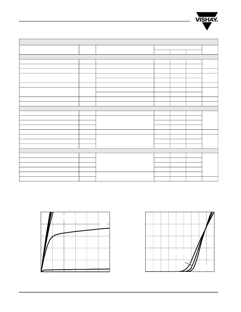
TYPICAL CHARACTERISTICS 25 °C, unless otherwise noted
20
V GS = 10 thru 5 V
20
16
12
8
4V
16
12
8
T C = 125 °C
4
4
25 °C
0
3V
0
- 55 °C
0
1
2
3
4
5
6
0.0
0.5
1.0
1.5
2.0
2.5
3.0
3.5
4.0
4.5
www.vishay.com
2
V DS - Drain-to-Source Voltage (V)
Output Characteristics
V GS - Gate-to-Source Voltage (V)
Transfer Characteristics
Document Number: 73234
S-80642-Rev. B, 24-Mar-08
发布紧急采购,3分钟左右您将得到回复。
相关PDF资料
SI2307BDS-T1-GE3
MOSFET P-CH 30V 2.5A SOT23-3
SI2307CDS-T1-E3
MOSFET P-CH 30V 3.5A SOT23-3
SI2308BDS-T1-E3
MOSFET N-CH 60V 2.3A SOT23-3
SI2312BDS-T1-GE3
MOSFET N-CH 20V 3.9A SOT23-3
SI2315BDS-T1-GE3
MOSFET P-CH 12V 3A SOT23-3
SI2335DS-T1-GE3
MOSFET P-CH 12V 3.2A SOT23-3
SI2367DS-T1-GE3
MOSFET P-CH 20V 3.8A SOT-23
SI2377EDS-T1-GE3
MOSFET P-CH 20V SOT-23
相关代理商/技术参数
SI2306DS
制造商:Vishay Siliconix 功能描述:
SI2306DS-T1
功能描述:MOSFET 30V 3.5A 1.25 RoHS:否 制造商:STMicroelectronics 晶体管极性:N-Channel 汲极/源极击穿电压:650 V 闸/源击穿电压:25 V 漏极连续电流:130 A 电阻汲极/源极 RDS(导通):0.014 Ohms 配置:Single 最大工作温度: 安装风格:Through Hole 封装 / 箱体:Max247 封装:Tube
SI2306DS-T1-E3
功能描述:MOSFET 30V 3.5A 1.25 RoHS:否 制造商:STMicroelectronics 晶体管极性:N-Channel 汲极/源极击穿电压:650 V 闸/源击穿电压:25 V 漏极连续电流:130 A 电阻汲极/源极 RDS(导通):0.014 Ohms 配置:Single 最大工作温度: 安装风格:Through Hole 封装 / 箱体:Max247 封装:Tube
SI2306DS-T3
制造商:Vishay Intertechnologies 功能描述:30V, N-CHANNEL, 94mohm 4.5V RATED TR
SI2307
制造商:未知厂家 制造商全称:未知厂家 功能描述:30V P-Channel Enhancement-Mode MOSFET
SI2307BDS
制造商:VISHAY 制造商全称:Vishay Siliconix 功能描述:P-Channel 30-V (D-S) MOSFET
SI2307BDS-T1
制造商:VISH 功能描述: 制造商:VISHAY/SILICONIX 功能描述:
SI2307BDS-T1-E3
功能描述:MOSFET 30V 3.2A 1.25W RoHS:否 制造商:STMicroelectronics 晶体管极性:N-Channel 汲极/源极击穿电压:650 V 闸/源击穿电压:25 V 漏极连续电流:130 A 电阻汲极/源极 RDS(导通):0.014 Ohms 配置:Single 最大工作温度: 安装风格:Through Hole 封装 / 箱体:Max247 封装:Tube
